为什么时钟树上要用clock inverter(min pulse width check)

Min pulse width定义
最小脉冲宽度检查可确保时钟信号的宽度足够宽,以便采集到正确的数据,保证设计功能。即为了获得稳定的输出,需要确保时钟信号宽度至少达到某个“最小宽度”。比如lib中就对寄存器Flipflop的CLK pin有min pulse width的check。
High pulse width
If you need a formal definition of the term, it is the interval between the rising edge of the signal crossing 50% of VDD and the falling edge of the signal crossing 50% of VDD.
Low pulse width
If talking in terms of low signals, it is the the interval between falling edge of the signal crossing 50% of VDD and the rising edge of signal crossing 50% of VDD.
以下图为例,一个时钟信号CLK,经过六级普通buffer(各自的rise time和fall time是不相同的)到达一个寄存器的CK 端。我们来计算下high pulse width,low pulse width以及判断是否存在min pulse width违例(uncertainty:80ps Reg ck pin requirement min pulse width:0.420ns)。
")
High pulse width = 0.5 (0.049-0.056) (0.034 -0.039) (0.023-0.026) (0.042-0.046) (0.061 – 0.061) (0.051-0.054) = 0.478ns
Low Pulse width = 0.5 (0.056 – 0.049) (0.038 – 0.034) (0.026 – 0.023) (0.046 – 0.042) (0.061 – 0.061) (0.054 – 0.051) = 0.522ns
high pulse width = 0.478-0.080 = 0.398ns (小于0.420ns)
因此,存在min pulse width violation。
Min pulse width检查方式
Liberty文件
Liberty文件中对寄存器的CLK pin和reset pin均有一个默认的min pulse width check值。在STA分析时工具会自动载入进行check。如图1所示,index_1为input transition。
")
图1 lib中min_pulse_width属性定义
SDC约束
除了采用lib文件中默认的min pulse width值check外,我们还可以通过如下SDC命令来设置特殊的约束条件。
set_min_pulse_width -high 2 [get_clocks clk]
set_min_pulse_width -low 1 [get_clocks clk]
理想clock buffer/inverter的特性
Equal rise and fall times
Less delay variations with PVT and OCV
Clock buffer能够驱动较长的net以及更多的fanout
普通buffer如何导致pulse width violation?
图2显示了Wp = 100nm&Wn = 100nm的Buffer电路的示意图。β比率(PMOS的宽度与NMOS的宽度的比率)由于NMOS的迁移率高于PMOS,因此上升时间大于下降时间。这个结论是根据电流公式得出的,不懂的请移步模拟电路查阅。
")
图2 Unbalanced Buffer电路原理图
这里的每个buffer都需要更多的时间来充电(相比放电过程)。输入为占空比为50%的周期为4ns的脉冲信号。当时钟信号通过buffer chain传播时,脉冲宽度如下图4所示减少相当多。最后一个buffer的输出具有相同的周期,但占空比发生了变化。在最坏的情况下,这种情况可能会小于设计所需的脉冲宽度(最小脉冲宽度)。
")
图3 Unbalanced Buffer Chain
")
图4 pulse width reduction
Balanced buffers have equal rise and fall time
为了使得buffer的上升和下降时间一致,PMOS的宽度应该约为NMOS的两倍(具体倍数关系取决于工艺)。Balance buffer电路结构图如图5所示。图6为一堆balanced buffer级联的buffer chain的输出波形。从输出波形看到,当我们在clock path上使用这种balanced buffer,输出时钟信号周期未发生变化且占空比仍然为1:1,即不会出现pulse width violation。
")
图5 balance buffer电路结构图
")
图6 Balanced Buffer Chain 输出波形
unbalanced inverter有没有min pulse width问题?
如果在时钟路径中使用偶数个反相器,一对反相器上升和下降时间会相互补偿,所以脉冲宽度并不会改变。所以反相器输出不会导致脉冲宽度违规。
图7所示为一个反相器的电路结构图。其中Wp = 100nm,Wn = 300nm。根据P管和N管的尺寸,我们得知上升时间比下降时间小得多。
")
图7 Unbalanced 反相器原理图
图8所示为一个十级反相器级联的电路图。图9为第九级和第十级反相器输出波形图。从图中可以得知,unbalance inverter同样也不会导致min pulse width问题。
")
图8 unbalanced inverter chain
")
图9 第九级,第十级反相器输出波形图
所以,在做时钟树综合时,我们往往选用clock inverter来长clock tree。
数字后端设计实现之时钟树综合实践篇
一网打尽时钟树综合Clock Skew
时钟树综合(clock tree synthesis)基础篇
思考题:
如果用clock buffer来长clock tree呢?各自的优缺点分别是什么?clock buffer和普通buffer的优缺点各是什么?(答案均在本文中)
小编知识星球简介:
在这里,目前已经规划并正着手做的事情:
ICC/ICC2 lab的编写
基于ARM CPU的后端实现流程
利用ICC中CCD(Concurrent Clock Data)实现高性能模块的设计实现
其他内容待定
在这里,各位可以提问(支持匿名提问,提问从此不再害羞),小编会在24小时内给予解答(也可以发表你对某个知识点的看法,项目中遇到的难点,困惑或者职业发展规划等)。
相关文章


最新文章
-

准备好没有《药性歌括400味》今天看看哪四味
12小时前 -
图11 完成“空间转换”后的解剖展示
14小时前 -
一、胃肠型感冒的症状
14小时前 -

夏季喝什么药膳粥好
14小时前 -

论勇 第五十——
14小时前 -

二、关于正踢腿
14小时前 -
倪海厦伤寒杂病论心法笔记(十一)
14小时前 -

抑郁症,不但能治好,而且非常好治!也不光是抑郁症,包括很多心...
14小时前
热门文章
-

舌头好看,病就好了。一个治腻苔的中成药
1周前 -
王铎草书简析
6天前 -
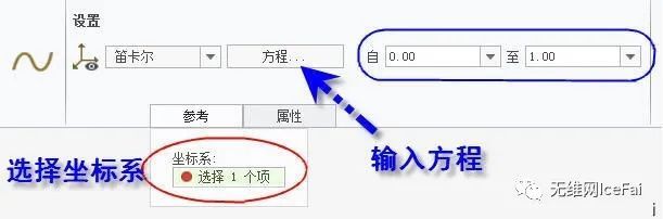
精华收藏!深入ProE和Creo圆角的原理和应用(一)
1周前 -

五分钟等效一万步的走路法
1周前 -
鲁藻:兰花画家的坚韧与传世之美
1周前 -

《淋证(泌尿系、结石)》——胡希恕
1周前 -

体内有癌,身体3处会发“黑”
1周前 -

风流后主李煜:艳词背后透出来的其实是他悲戚的人生
1周前


有话要说...